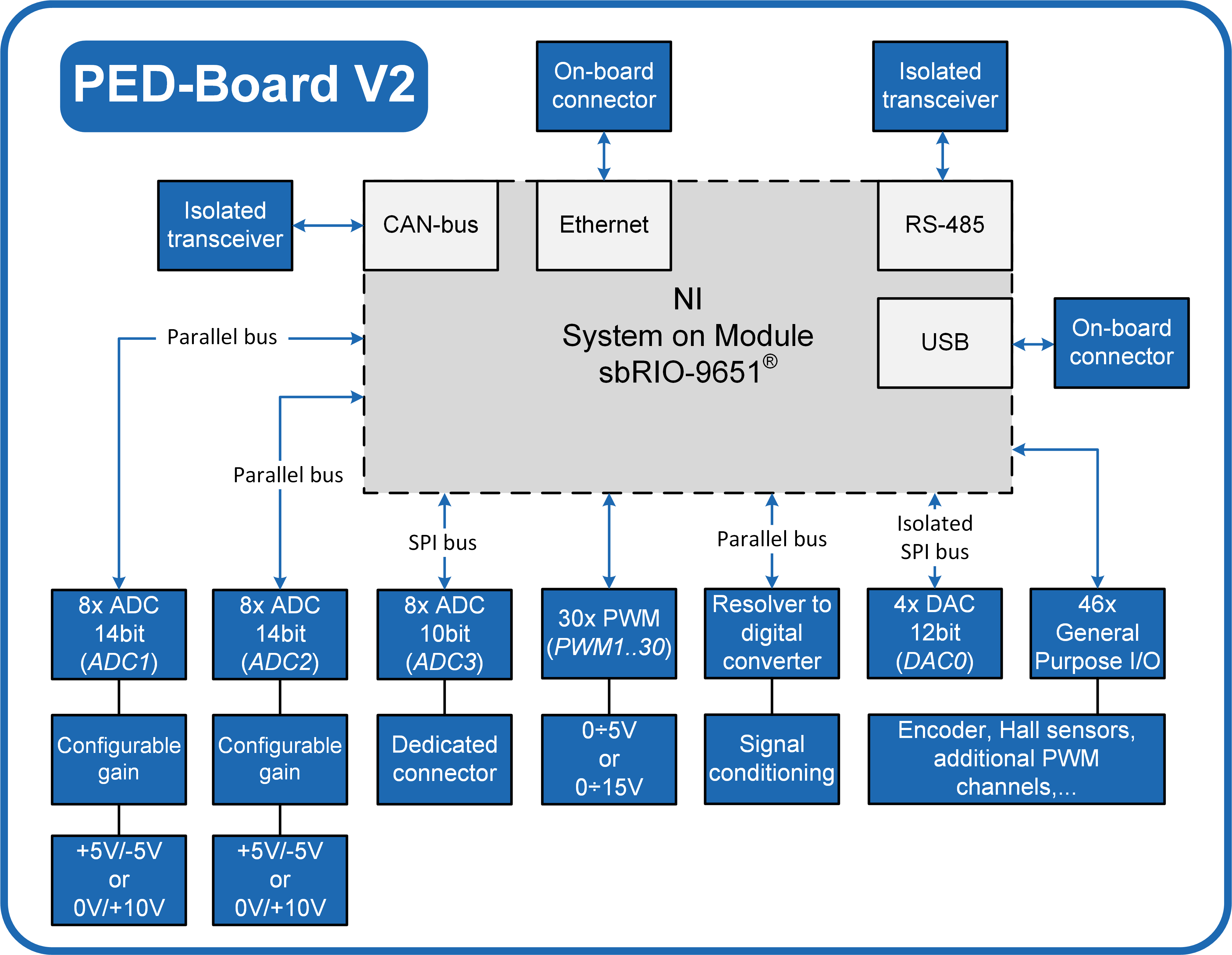
FUNCTIONAL BLOCK DIAGRAM
FEATURES
30 x PWM channels
- 0÷15 V or 0÷5V selectable voltage swing
- Direct LED driving capability for optocoupled gate driver
- Additional PWM channels available through the Digital I/O interface
14-bit ADC, 8 Channels
- Simultaneous sampling
- 1.45 μs conversion time, 8 channels
- Differential input
- Configurable gain (each channel)
- Second order low-pass Butterworth active filter with
configurable cut-off frequency (default 20 kHz)
14-bit ADC, 8 Channels
- Simultaneous sampling
- 1.45 μs conversion time, 8 channels
- Differential input
- Configurable gain (each channel)
10-bit ADC, 8 Channels
- Up to 200 kS/s
12-bit DAC, 4 Channels
- Digital-to-analog converter with 5 μs settling-time
- Isolated, no ground loops
Resolver interface
- Fully configurable electrical interface
- Speed and position measurement
- Resolver fault detection
46 x Digital I/O
- Hall-effect position sensors interface
- Encoder interface
- Relay control
- Additional PWM
- General purpose I/O
1 x 10/100/1000 base-T Ethernet port
- Auto-negotiated, half/full-duplex
- Programming, debugging and operation
1 x RS-485
- Isolated transceiver
- Half-duplex and full-duplex communication
- On-board terminator resistor
1 x CAN-bus
- 2.0A and 2.0B support, up to 1 Mbit/s
- Isolated transceiver
- On-board terminator resistor
USB port
Dedicated LabVIEW drivers and demo programs have been developed to completely support the user in the application software design stage. Each peripheral is fully supported by the LabVIEW CLIP and/or a specific VI. Kernel programs are available for users with properly designed FPGA main scheduler, Real-Time target task, synchronization etc…